Semiconductor packaging technology is a critical环节 in the electronics manufacturing process, serving as the bridge between delicate silicon dies and the external world. It involves enclosing and protecting semiconductor chips, providing electrical connections, ensuring thermal management, and enabling integration into larger systems. As semiconductor devices continue to miniaturize and increase in complexity, packaging technologies have evolved significantly to meet the demands of high performance, low power consumption, and reliability. This article explores the fundamentals of semiconductor packaging, key technologies, challenges, and future trends, providing a comprehensive overview of this essential field.
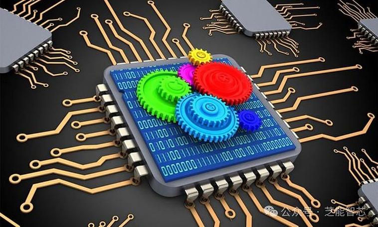
Semiconductor packaging begins after the silicon wafer is fabricated and diced into individual dies. The primary goal of packaging is to protect the fragile die from mechanical stress, moisture, and contaminants, while establishing reliable electrical connections between the die and the printed circuit board (PCB). Early packaging technologies, such as through-hole packaging (THP), used leads that passed through holes in the PCB. However, the shift to surface-mount technology (SMT) in the 1980s revolutionized packaging by enabling smaller, lighter components with better thermal and electrical performance. Today, advanced packaging techniques like chip-scale packages (CSP), wafer-level packaging (WLP), and 3D stacking are driving innovation in industries ranging from consumer electronics to high-performance computing.
One of the most widely used packaging technologies is quad flat no-lead (QFN), which offers a compact footprint and excellent thermal dissipation. QFN packages have exposed pads on the bottom that directly contact the PCB, improving heat transfer and reducing electrical inductance. Another popular type is the ball grid array (BGA), which uses an array of solder balls on the bottom of the package to connect to the PCB. BGAs provide higher pin counts and better signal integrity than older packages like dual in-line packages (DIP), making them ideal for complex integrated circuits (ICs) such as microprocessors and FPGAs. For ultra-miniaturized applications, wafer-level packaging (WLP) processes the entire wafer before dicing, resulting in packages that are nearly the same size as the die itself. WLP is commonly used in smartphones, wearables, and other space-constrained devices.
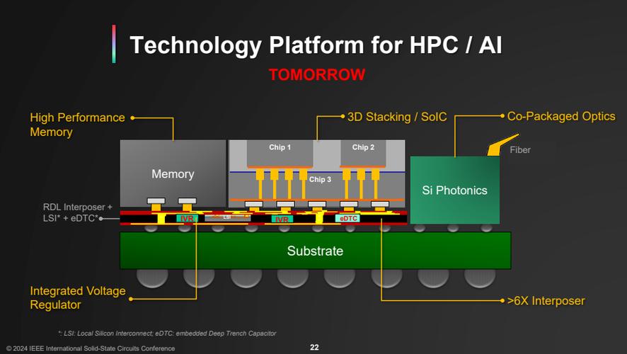
The demand for higher performance and integration has led to the development of 3D packaging technologies, which stack multiple dies vertically to reduce interconnect lengths and improve signal speed. Through-silicon via (TSV) technology is a key enabler of 3D packaging, allowing vertical connections through silicon dies. TSVs offer shorter signal paths, lower power consumption, and higher bandwidth compared to traditional wire bonding, which connects the die to the package using fine wires. 3D stacking is widely used in memory devices like high-bandwidth memory (HBM) and in multi-chip modules (MCMs) for AI and high-performance computing. Another advanced technique is fan-out wafer-level packaging (FO-WLP), which redistributes die pads to create a larger interconnect area, enabling higher I/O counts and better electrical performance.
Thermal management is a critical consideration in semiconductor packaging, as high power densities can lead to overheating and reduced device reliability. Advanced packaging solutions incorporate thermal vias, heat spreaders, and thermal interface materials (TIMs) to dissipate heat efficiently. For example, flip-chip packages, where the die is flipped and connected directly to the substrate, offer better thermal performance than wire-bonded packages. Additionally, packages with exposed pads or metal lids can enhance heat dissipation, particularly in high-power applications like power electronics and automotive systems.
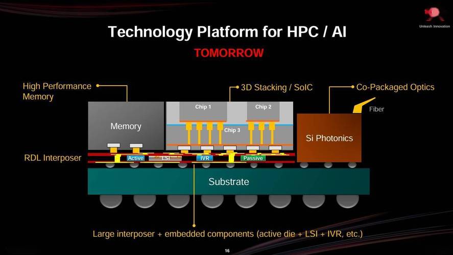
As the semiconductor industry moves toward smaller process nodes and heterogeneous integration, packaging technologies continue to evolve. System-in-package (SiP) technology integrates multiple dies, passive components, and even sensors into a single package, enabling compact and multifunctional solutions. SiPs are widely used in smartphones, IoT devices, and automotive electronics, where space and performance are critical. Another emerging trend is the integration of packaging with silicon photonics, which uses optical interconnects to achieve higher bandwidth and lower power consumption in data centers and high-speed communication systems.
Despite advancements, semiconductor packaging faces several challenges. One major issue is the increasing complexity of packaging processes, which require precise control and advanced materials. As dies become smaller and packages more intricate, defects such as cracks, delamination, and solder joint failures become more common. Additionally, the demand for higher reliability in harsh environments, such as automotive and aerospace applications, necessitates robust packaging solutions. Cost is another challenge, as advanced packaging techniques like 3D stacking and TSVs are more expensive than traditional methods, requiring innovative manufacturing approaches to reduce costs.
Looking ahead, the future of semiconductor packaging will be shaped by the need for higher performance, miniaturization, and sustainability. Innovations in materials science, such as advanced substrates and low-k dielectrics, will enable faster and more efficient packaging. Artificial intelligence (AI) and machine learning (ML) will play a key role in optimizing packaging design and manufacturing, improving yield and reducing defects. Additionally, sustainable packaging practices, such as lead-free solders and recyclable materials, will become increasingly important as environmental regulations tighten.
In conclusion, semiconductor packaging technology is a rapidly evolving field that plays a pivotal role in the advancement of electronics. From traditional packages like DIP to advanced solutions like 3D stacking and SiP, packaging technologies continue to push the boundaries of performance, miniaturization, and integration. As the demand for smaller, faster, and more reliable devices grows, the industry will continue to innovate, ensuring that packaging remains a cornerstone of semiconductor progress.
FAQs
-
What is the difference between wafer-level packaging (WLP) and traditional packaging?
Wafer-level packaging (WLP) processes the entire silicon wafer before dicing, resulting in packages that are nearly the same size as the die. This approach reduces size, weight, and cost while improving electrical performance. Traditional packaging, on the other hand, involves assembling individual dies into packages after dicing, often resulting in larger sizes and higher costs. WLP is ideal for miniaturized applications like smartphones and wearables, while traditional packaging is used for larger, more complex devices. -
How does 3D packaging improve semiconductor performance?
3D packaging stacks multiple dies vertically, reducing interconnect lengths and improving signal speed. Through-silicon vias (TSVs) enable vertical connections between dies, lowering power consumption and increasing bandwidth compared to traditional wire bonding. This technology is particularly beneficial for high-performance applications like AI accelerators, memory devices, and multi-chip modules, where speed and efficiency are critical. By integrating multiple functions in a compact form factor, 3D packaging enables smaller, more powerful systems.


